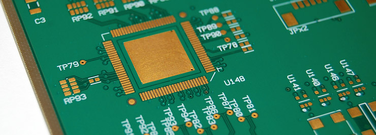
Multi-layer Printed Circuit Boards
The multilayer PCB is the development of the double sided PCB. With increasing complexity and density of components many designers were struggling to find the route and size required for modern instruments. Adding just a power and ground plane to the inside of the board allowed the components to be powered with just two plated holes to the inner layers rather than a track back to a power/ground point. Once the technology to multilayer PCBs was established, it was further developed to have additional signal layers inside. This allowed the designers to produce highly complex and compact circuits and further development of blind and buried via hole technology has pushed these limits even further. The highly complex PCBs now being offered allow high density packaging to the designer’s requirement and in line with the most complex components.
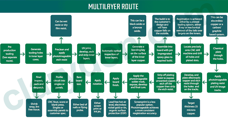
Click here to download the Multi-Layer PCB Route (PDF)
Our technical capability for this type of product is as follows:
Layer count Up to 32 layers
| Capability | Standard |
| Board Profiling | CNC RoutCNC ScorePierce Blank & Return |
| Minimum Trace width | 3 thou |
| Minimum Track Width to feature spacing | 3 thou |
| Smallest Finished Hole SizeMaximum Drilled Hole Size | 0.05mm6.0mm |
| Material Thickness | 0.35mm-6.4mm |
| Copper Thickness | Up to 6oz Cu |
| Max board size | 610mm x 610mm (Call if more needed) |
| Standard Surface finish | Lead Free Hot Air Level |
| Alternative finishes | Electroless Nickel / Immersion GoldSilverElectroless TinOrganic ( OSP )Hard Gold ( edge contact )CarbonPeelable |
| Bare Board Test | Bed of NailsSimultaneous 2 sided flying probe test |
| Solder mask | Photoimageable Resist with a wide range of colours. |
| Gold plate | Edge connectors Touch Pads |
For further details of any of the above specifications or for technical assistance on applying these specifications to your multi-layer printed circuit board needs please email, phone or Skype to our team who will be happy to help.