Single & Double Sided PTH PCB

Single Sided (Conventional) Circuit Boards
Although the single sided PCB is the most basic and the start point of printed circuit technology and indeed, the start point of the invention, it still plays a major role in the industry.
The PCB was invented to give a good mechanical base for components and by using printing to produce the tracks allowed repeatability of interconnections in volume.
It also means reliability of connections compared to hand wiring and another big benefit is ease of assembly production of an electronic device in volume.
In through hole device technology, it does have its limitations in interconnecting large numbers of components as all the tracks are on one side but it is a cheap way of gaining all the above benefits on more simple circuits.
Due to surface finishes like Lead free hot air level, Nickel Gold and organic surface protection, single sided boards can used for surface mount devices as well as through hole. Using this technology, although the PCBS are relatively simple, they can still be used in very complex devices. This is quite often apparent on LED technology.

Click here to download the Single Sided PCB Process Route.
Double Sided Printed Circuit Boards

The double sided “PTH” (plated through holes) PCB is the universal workhorse of the electronics industry. With increasing complexity and density of components many PCB’s need to use both sides of the Printed Circuit Board. This is more usually supplemented with plated-through-holes where the copper connections go right through the connecting holes to the opposite side of the board. These PTH Connections either form simple electrical connection between both sides of the PCB (Via Holes), or electrical connectivity and mechanical support for leaded components. This makes the double sided PTH PCB a much more physically robust item.

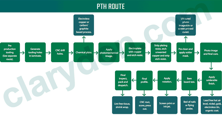
Click here to download the Double Sided PTH Process Route
| Capability | Standard |
| Board Profiling | CNC Rout CNC Score Pierce Blank & Return |
| Minimum Trace width | 3 thou |
| Minimum Track Width to feature spacing | 3 thou |
| Smallest Finished Hole SizeMaximum Drilled Hole Size | 0.05mm6.0mm |
| Material Thickness | 0.35mm-6.4mm |
| Copper Thickness | Up to 6oz Cu |
| Max board size | 830 mm x 420mm * Some circuits up to 2000mm Long |
| Standard Surface finish | Lead Free Hot Air Level |
| Alternative finishes | Electroless Nickel / Immersion Gold Silver Electroless Tin Organic ( OSP ) Hard Gold ( edge contact ) Carbon Peelable |
| Bare Board Test | Bed of Nails Simultaneous 2 sided flying probe test |
| Solder mask | Photoimageable Resist with a wide range of colours. |
| Gold plate | Edge connectors Touch Pads |
For further details of any of the above specifications or for technical assistance on applying these specifications to your needs please email, phone or Skype to our team who will be happy to help.
Our diagrams above for single sided PCB & double sided PTH PCB show the various processes and stages of manufacture required during the manufacture of these boards.
