Multilayer circuit board builds & sequential bonding
The first question must surely be why do we need to multilayer a circuit board? The answer is, as with a plated board, to allow more interconnection routes for the designer. As components have become smaller with more connections required, the routeing just gets more and more difficult.
When I used to explain plated through boards, I used the old school conundrum on drawing 3 blocks to represent Gas Water and electric. Then, 3 houses below. Now, connect each service to each house without crossing a feed. It can’t be done unless you go 3 dimensional which is as per the circuit boards. Draw the parallel with a single sided and double sided board and more.
That is as simple as I can make it.

Initially, the 4 layer board was a huge leap. The idea was, as there was so much power to distribute to every active component, it would be simple to add a power+ plane and a ground- across the whole board and just drill into pick up the relevant supply whilst having a clearance in the corresponding pad on the opposite plane, simple.
Then as progress pushed on, tracks were introduced to the inner layers and the 6 layer was developed. The tooling systems required for 4 layer were very basic as artworks could be aligned to holes on the inner layer. 6 layer pushed technology to design systems to align core to core and so registration became an issue. There are so many tooling systems it would take a long time to go through them but one easy one is to use rivets. The process would be thus:
- Drill tooling holes on all cores, probably 2 on each edge. Also, drill the pre preg.
- Use these to register the artworks for photomech etch resist and make the layer 2/3 and 4/5.
- Build the inner stack using rivets in 8 places.
- Build the complete stack and using a simple heat resistant tape over the selected inner layer target to allow location and removal of the outer copper post bonding to facilitate the drill registration holes being generated.

This is a very basic system but more modern ones include Xray, punches, self centre optics and more.
Sequential bonding (Buried via)
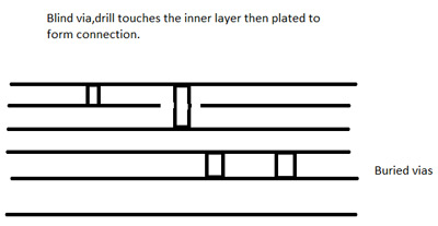
As the technology again increased with regard to component packaging, a requirement for buried and blind vias became apparent. My first introduction was with mobile telephone technology. This process involves making plated through board on thin cores then bonding them into the stack like an inner layer. I will keep it simple as that at the moment as to go through the process details would be unnecessary unless you are making them.
Blind vias
These are generated by depth controlled drilling, so, the drill machine will probably have laser measuring to locate the top of the board and drill through to the required inner layer. Again, this can be either layer closest to the surface or remove the copper on that layer to allow access to a lower layer.

The plating of blind vias is the challenge as there is no route through for the solution so knowledge of the plating process is critical.
Again, this is an appreciation of the processes rather than a definitive document. As always, I am happy to hear your views and comments. Email: Johnbarry@clarydon.com
Next month, a light look at factory life in PCB manufacturing, unless someone comes up with a better topic.
